PCB Designing in EAGLE
We decided to design the PCB in EAGLE. EAGLE is a software that allows users to design printed circuit boards while seamlessly connecting the circuit schematic diagrams, component placement, PCB routing, and comprehensive library content. Additionally, as an Autodesk software, EAGLE is highly integratabtle to Fusion 360, which allows us to continuously iterate our PCB design in the context of our yo-yo mechanical design.
Creating the Schematic:
Below is a screenshot of the schematic builder in EAGLE. At the high-level, here you:
- add electronic parts (parts shown in red)
- wire the parts together (wires shown in green)
- name the parts (part names shown in grey)
Creating the Board:
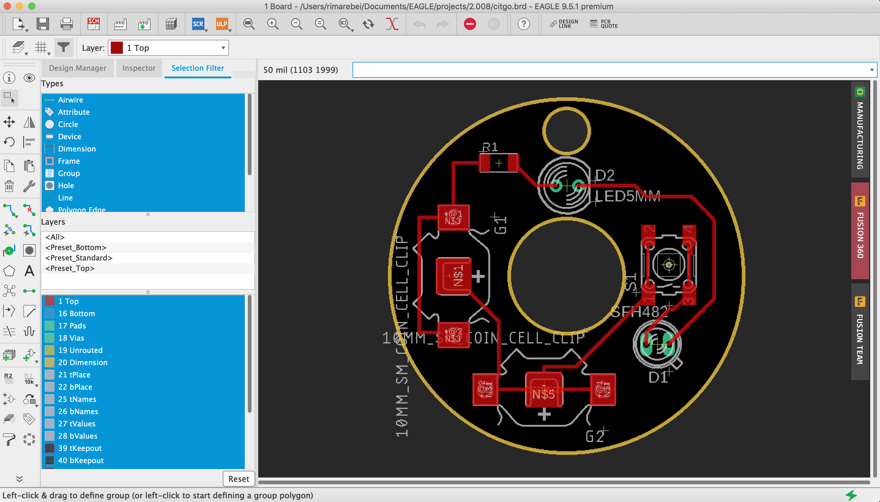
Below is a screenshot of the board builder in EAGLE. EAGLE exports all of the parts and wire connects from the schematic builder into this interface. This is what the manufacturers will see and what you make the CAM after. Each PCB has multiple layers that hold different information. Some of the important layers I used for this design are:
- 1 Top (shown in red): These are all the wires and pads for the surface mounted parts. The pads will be placed at the top of the
- 20 Dimensions (shown in yellow): Here is where you draw the board outline and any holes. When machined, anything in the Dimensions layer will be cut completely through.
- 18 Vets (shown in green): These are the the the holes that will be drilled for the through hole parts (the two LEDs in this case)
- 21 tValues (shown in grey): These are the values of any parts that will be silkscreened when the PCB is manufactured. The value of the resistor will be silkscreened.
- 21 tNames (shown in grey): These are the part names so when assembly comes, our team will know what part goes where.
Below is a screenshot of our first PCB design. Originally, the PCB was going to lay at the bottom of the body of the yo-yo, and then held together (to stop from spinning) with a screw that would be screwed in to the bottom of the body. Ultimately, we decided not to go with this design, because mechanically it would be a lot harder to press the push button switch by the triangle piece when it is not in the center of the PCB.


Comments
Post a Comment